Kobelco LEO Division
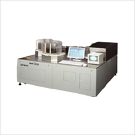
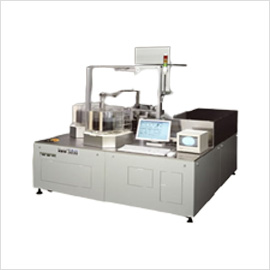
LTA (for FPD) / LTA (for Wafer)
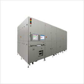
Lifetime Measurement System
- Comply with JEIDA Standard (53-1997)
- Multi-layer wafer lifetime
- High-sensitivity, high speed
- Iron concentration measurement
- Ample measuring/indicating modes
- OX film/silicon interface evaluation
- Evaluation of p-Si and Oxide layer of LCD
- Evaluation of SiC
LEP
Edge Profile Monitor
- Complying with Method-B of the Standard in measuring edge shape (ASTM-F928-93)
- High precision
- Various measurement items
- Various models
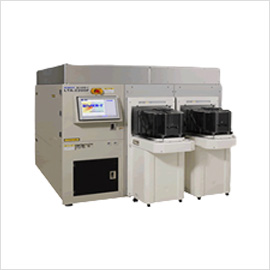
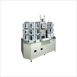
SBW / LBW
Bow/Warp Measurement System
- High-speed, high-precision
- Free selection of measurement plane and reference plane
- Various data display
- Multiple measurement items (Bow, Warp, Thickness, TTV)
- Measurements in various processes
- Compact, reasonable price
- Multi-Port (LBW)
- LBW + Magic Mirror System
- Fine concave/convex visualization
- Wide detection coverage
- Magnification selection
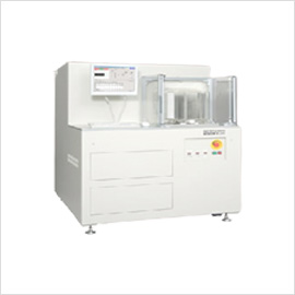
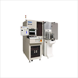
LER

Egde roll off Measurement System
- Simultaneous measurement of the front and back sides
- Measurement of both mirror finished surface and rough surface
- High precision, High repeatability
- Various data display (2-D / 3-D profiles)
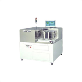
LRW
Wafer Sorter
- Order made
- Various sensors
- Unrestricted construction
- User friendly software
EPM
Bonding Evaluation / Edge Defect Inspection System
- Bonding Evaluation Outline
- Various Edge Shape
- Notch Deviation